Design Idea:
Optical Sensor Interfacing
Highlighted features:
- Low standby current consumption
- Long life expectancy
- Only one added transistor = low parts count
- Fast and linear operation
- Analog (linear) low-impedance output
- Alternatively Schmitt-trigger digital output
- Adaptable for different operating voltages (>= +3.3V)
- Adaptable for different sensors with different CTR
- Suitable for both transmissive and transflective sensor types
- Especially transflective sensors benefits from the analog and linearized operation making it possible to design adaptive sensing and an ADC with software to XXX
Background
Slotted transmissive (or transflective) optical sensors are widely used in many applications. The interface is very simple; just ensure that an ample amount of current flows through the emitter, and properly load (but lightly) the sensor side. This requires as simplest only two resistors, see Fig.1.
However, this basic circuit - in its simplicity - has some downsides:
- It consumes current constantly, and at a fairly high level (10...20mA). Especially in multichannel reflective applications the total current can be substantial.
- You could chop the power supply to all sensors to save power, but during idle periods, the sensors are non-functional.
- The output is actually an analog output having slow fall and rise times and often requires a Schitt trigger follower.
- The operating point is very much dependent on the current transfer ratio (CTR) of the sensor.
- Due to the constantly on and relatively high emitter current (especially in transflective sensors), the sensor will degrade over time (reduced sensitivity). This can be overcome by increasing the IR-emitter power even further.
- The sensor output is high impedance (RL) and especially long wires will pick up noise.
This idea
This variation of the sensor interface has the following benefits:
- The current consumption is minimized when the transmissive sensor slot is not obstructed, saving current in applications where the slot is only occasionally obstructed (typical edge or limit sensors).
- Likewise - current consumption is lowest when the transflective sensor is in close proximity to a target, saving current (and sensor lifetime) in applications where the reflective surface is only occasionally removed from the sensor vicinity.
- High positional sensing precision can be achieved since the output (in the basic configuration) is an analog signal that correlates to the amount of light transferred from the emitter to the receiver. Therefore the position of the object (and how much it covers the sensor beam) can be detected with much higher precision compared to the typical application in Fig.1.
- The signal output is low impedance.
- By adding another transistor and two resistors the output can be converted to a digital signal with an internal Schmitt trigger function, resulting also in fast rise and fall times (<1µs) while still keeping the other benefits.
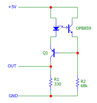
The principle of the proposed circuit
The trick is to run the sensor in a local negative feedback mode. In this configuration, the IR emitter gets just as much current as is required to keep the sensor's output current constant - and at a predefined level. If this equilibrium cannot be held (ex. when no signal is hitting the receiver) then the transmitter current will increase but only to a safe predetermined level.
The phototransistor output is not used as the output, instead, the current dumped in to the IR-emitter is converted to a voltage and this is used as the signal output. This analog signal can directly be interfaced with an ADC (in an MPU) for very fine and high-precision detection. This signal is a precise representation of the current going into the IR emitter - the current needed to keep the circuit in its equilibrium. This circuit arrangement where the IR-emitter is connected to the PNP-transistor's emitter side also keeps the voltage across the phototransistor fairly constant and high enough to ensure linear operation. At the same time the phototransistor's Miller (and other capacitance's) influence is effectively cancelled, increasing the overall speed even when running at relatively low phototransistor currents. Please note that this strong negative feedback also linearizes and widens the optical sensing gap of the sensor.
The question arises - why would you like to shallow the slope (or gain) of the sensor and have a wider optical sensing gap, since you just want to sense reliably an edge in a slotted sensor, or a certain distance in a tranflective sensor? When you use an ADC input to sense the sensor's output voltage this has no relevance. On the contrary - now that the edge sensing area is wider (and linearized) you can fine-tune the sensing point in software - and probably also avoid a mechanical adjustment of the sensor itself in applications that need very precise (and maybe user fine-tunable) reference sensing! However, this is not something I have tested but the sensing area is extended so this is feasible. Using the ADC also gives you better diagnostics - a missing or malfunctioning sensor can easily be detected without additional hardware.
Detailed explanation
Only one general-purpose PNP transistor is added to the original circuit to facilitate this improved behavior. Any small signal transistor with hfe>200 will do, BC327 is one good candidate. Due to the nature of the circuit, the output voltage can never exceed VCC-VF[diode]-VSAT[Q1]. In a +5V application, this is typically +3.75V, in an +3.3V circuit the maximum voltage is 2.05V. This is usually not a problem when feeding an ADC input. TTL-compatible digital inputs can also be driven with such a low signal. If a true digital signal with a full voltage swing is needed, such a circuit is presented at the end of this article.
Dimensioning of the circuit
Here are simple some steps for dimensioning the two resistors. In this example, the transmissive OPB859 sensor is used. This slotted coupler has a CTR of only 0.0125 (1.25%) and is, therefore, trickier to use than many others. However, this is a quite typical CTR for a transflective sensor so this is a good worst-case example.
- Check the minimum guaranteed CTR from the datasheet. In this case, it's 1.25% (20mA/250uA - from page 8 in the datasheet).
- Check the recommended IR-emitter operating current. For the OPB859 it is 20mA. More power can even be saved since this circuit works excellently (and is still fast) with only one-quarter of the recommended IR-emitter current. We opt for 20mA/5=5mA. You can dimension the circuit for higher operational currents, but there is nothing to benefit from doing so.
- Check the IR-emitter forward voltage at the rated forward current (5mA). In this datasheet there is no curve so we approximate it to be 1.1V.
- Now we can calculate R1 which determines the maximum current via the IR-emitter:
(VCC-VF[diode]-VSAT[Q1])/5mA. Since VCC is +5V we get:
(5-1.1-0.2)/5mA = 740Ω - we select a standard 680Ω value. This will give 5.5mA as the maximum current. - To guarantee that the transistor reliably can deliver 5.5mA we need at least (5mA/200) 27.5µA at the base.
- The beautiful thing with this circuit is that base sits fairly stable at VCC-VF[diode]-Vbe[Q1]. With+5V as the supply we get 5-1.1-0.6=3.3V as the base voltage. This stays fairly stable and varies due to the dynamic resistance of the IR-emitter and the temperature variation of the VBE of Q1. Since both are relatively stable the maximum variation is practically <100mV, so R1 actually acts as a constant current sink. 3.2V/27.5µA gives 116kΩ as the maximum value for R2. We select 100kΩ. This fairly stable current must be overcome by the phototransistor for the transistor to regulate the IR-emitter current. Thus this current also determines the minimum idle current via the IR-emitter and we would like to keep this as small as possible. Going too low can give problems if there are strong IR-light sources within the view of the optosensor's phototransistor. Well, you can't go below 27.5uA (the minimum required base current) and with the worst case CTR of 1.25% this will result in an IR-emitter current of 27.5uA*1/CTR= 2.2mA to keep the control loop happy. XXXXXX
What if you need a real digital signal with fast rise and fall times directly from the sensor?
In many applications, you just need a digital input that reflects the status of the sensor (on/off), or you cannot use an analog input.
With the addition of only one transistor and two resistors, you can convert the sensor's analog output to a digital output with a built-in Schmitt trigger operation. The low power consumption is preserved, as well as the speed and precision. By varying one resistor's value the hysteresis can be tailored. And there is no need to add an additional Schmitt trigger to square up the signal since the sensor already produces a good digital signal, with low output impedance and symmetrical rise and fall times.
NOTES:
Due to the fact that the sensor function needs only 3 wires, and the sensor itself is happy also with 3 wires (you can combine IR-LED anode and phototransistor collector) it is possible to add the extra circuitry either at the main PCB - or at the sensor. If the sensor is close to the PCB you can wire it directly and build the circuitry on your main PCB. t is strongly recommended to build the circuitry on the same small PCB close to the sensor if the sensor is further away.
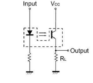
Fig.1 Basic and simple interface of a transmissive (or transflective) optical sensor.
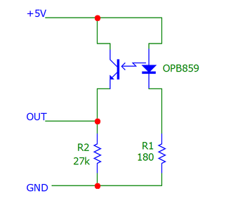
Fig.2 Typical application using the OPB859 slotted optosensor. Note that the wiring can be alternatively done with the resistors at the +VCC side. Function is the same.
Fig.3 Improved sensor with added transistor Q1. Check the text for functional explanation.
Background
Slotted transmissive (or transflective) optical sensors are widely used in many applications. The interface is very simple; just ensure that an ample amo
Copyright @ DEXTREL / 2022 / All Rights Reserved