Design Idea:
Base current error compensation
in current sources
A MOSFET is an excellent choice as the pass transistor when designing a good quality current source for higher output currents. The gate current is negligible and not degrading the accuracy of the current source. Also, its power gain is close to infinity.
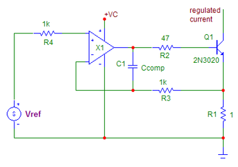
However, a power MOSFET has high parasitic Ciss and Coss capacitances that limit the output impedance at high frequencies. Power bipolar transistors with low hfe are fast and have radically lower output capacitances than equally sized power MOSFETs. However, a bipolar transistor-based regulated current source (as shown in Fig.1) suffers from accuracy errors due to the base current flowing into the output current measurement resistor.
The base current varies with the collector current and changing hfe, which in turn depends on the transistor’s production tolerances, temperature, and transistor c-e voltage. Using a Darlington transistor would increase the current gain and reduce the error, but the high-frequency behaviour would become limited and make the transistor selection more constricted. Super-beta power transistors are rare, have typically lower ft and are also more expensive.
In other words, even if the bipolar transistor has higher output impedance at higher frequencies it is not the first choice in high-precision current sources due to the base current-induced error. This could be compensated by measuring the output current at the collector side but would increase complexity and also reduce the current source's output impedance.
This Design Idea presents a simple and effective way of reducing the base current error by at least two orders of magnitude using standard (1%) tolerance components, enabling the of use low hfe bipolar transistors in precision current sources. The basic idea is to measure the base current and add a proportionally scaled error term to the reference voltage to compensate for the error.
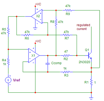
One possible implementation is shown in Fig.2. The current regulator is still the same as in Fig.1. A second op-amp X2 and resistors R6-R9 forms a differential amplifier measuring the base current by measuring the voltage across R2. This error voltage is scaled and added to the reference voltage using resistors R4 and R5.
Since the differential amplifier is referenced to the upper end of the current shunt resistor R1 (and not to ground) the error voltage is itself referenced to the reference voltage. This preserves the scaling; the output current is still calculated as Vref/R1. As a result, the voltage regulated across R1 represents the desired output current added with the transistor’s base current. The transistor inherently “subtracts” the base current and the resulting collector current is now virtually error-free.
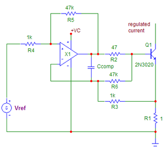
After having designed this circuit and looking at the equations and the added complexity it soon became obvious that the schematic can be simplified. Both X1 and X2 can be combined still preserving the error-correcting function. Actually, you just need to add two resistors to the original schematic in Fig.1 to achieve the same effect! The final circuit is shown in Fig.3.
To better understand the circuit’s operation, think of it as a voltage regulator that tries to regulate a voltage equal to Vref across R1. If the base resistor R2 would be a short circuit then it can easily be seen that R5 and R6 do not influence the operation. Whatever common-mode error they produce is cancelled out. Since R2 is not a short circuit but a known resistance, there is a voltage across it that represents the base current. This voltage is fed back to the input via R5/R4 divider thus increasing the regulated voltage across R1 with the same ratio. If this ratio is the same as R2/R1 then the voltage regulated across R1 includes an error term that effectively cancels the base current. Assuming that R3=R4 and R5=R6 then the output equation is:
Since the base current Ib shows up in the formula twice with opposite signs the formula simplifies back just to:
The base current-induced error is typically reduced to about 1/100th from the initial level using standard 1% tolerance resistors. A power transistor (with typical hfe of 25 and no base current compensation) would cause a full-scale current error of 4%.
The circuit corrects this to 0.04%, equaling an effective hfe of 2500! Perfect matching would result in an immeasurable base current error. For proper operation, the following resistor ratios must be fulfilled:
R2/R1=R5/R4; R5=R6; R3=R4; R5>>R4; R3>>R1.
The op-amp must have an input common-mode range that includes the negative rail. The op-amp bias current-induced errors are well balanced since the resistances at both inputs are equal. The minimum +VC voltage depends on the current sourcing saturation behaviour of the op-amp and the combined worst-case voltage drop across the Q1 base-emitter junction, R1, and R2. The maximum output current depends on the worst-case hfe of the transistor multiplied by the minimum worst-case current output from X1. The absolute accuracy and final response depend on the selected op-amp and resistor tolerances.
This circuit works equally well using two transistors in a Darlington configuration. The additional hfe further improves the operation. With this circuit, you can even add a speeding-up base-emitter resistor across the output transistor's b-e junction and the current in this resistor will NOT introduce an error to the current source output.
The reference voltage can be either fixed or adjustable. For the smallest possible error, the reference voltage's output impedance should be fairly low due to the small feedback current induced via R5. If needed, resistors R3 to R6 can be scaled proportionally higher to reduce this effect.
Amazing what you can achieve with only two additional resistors in an already simple circuit!
Fig.1 A typical fast bipolar transistor current sink but with base current-induced error, the nominal output current is:
Iout= (Vref/R1)-Q1Ibe
Fig.2 The same circuit as in Fig.1, but with added base current error compensation. With perfect resistor matching the output current is simplified to: Iout= (Vref/R1)
e
Fig.3 The FINAL simplified base current corrected current sink, adding only two resistors to the original schematic in Fig.1. Output current still reduces to: (Vref/R1)
The idea as published in EDN magazine
JULY 6, 2006. Click on the pop-out icon to read it in full size.
Copyright @ DEXTREL / 2022 / All Rights Reserved


