60W Ultra-Simple Audio Power Amplifier
Highlighted features
- Simple but powerful 60W amplifier
- Uses easily available (junkyard) components
- Overload protection
- No turn on-thump (no need for output relay)
- Low parts count, low-cost BOM
- Low hum and noise
- Input impedance: >30kohm
- Bandwidth @40W: 10Hz-30kHz (-1.5dB)
- SNR: >94dB
- Gain: +34dB
- Damping factor: >50
- THD@1kHz: <0.05% @ 40W into 6 ohm
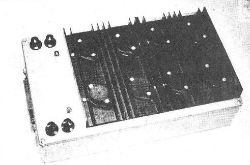
Fig.1 Compact 4-channel version built into an aluminium casted box.
Main Specifications
This audio power amplifier is both simple and sturdy, with its components striking a good balance between performance and cost. Its overall performance is more than adequate for home use. All of the components used are common and can easily be found in a component junkyard. The amplifier is designed to work with 8-ohm loads and can deliver 40W of continuous power with distortion levels of less than 0.05%. It can also handle 6-ohm loads without issue. However, it is not recommended for loads less than 6 ohms. The original instructions for this project were in Finnish, but I have translated the most important parts for you here.
Design background
This design has many similarities with the old and popular Texan amplifier from 1972. The output stage consists of a clever output stage with voltage gain. It uses complementary, feedback or "compound" - or "Sziklai" pair - transistors. The output power transistors' Q6 and Q7 Vbe voltage (and its variation due to temperature changes) have a minuscule effect on the idling current. The control of the output stage idle current is fairly simple since temperature feedback from the power transistor heatsink is not needed. It is enough that Q1 and Q4 (which could also be Q1 and Q2) are thermally connected to each other.
Electronic short-term overload protection is also added, and the maximum output current is reduced by limiting the maximum base current to the power transistors. The power transistors have a relatively low hfe so there is very little risk of destructing the output stage during brief overloads.
The Texan design had a fuse at the output. Fuses cause additional distortion at lower frequencies. Electronic protection circuits also add some distortion but have some advantages over fuses. The overload protection in Texan was not fast enough to protect the output transistors during brief overloads. Let's look at the schematic (TULO means input):
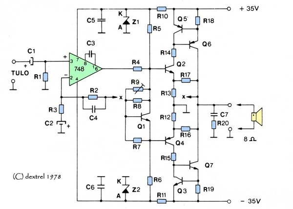
Fig.2 Complete schematic of one channel.
Output Stage
The output stage voltage gain is determined by the ratio of R17/R13 (and R16/R12). The overall resistance at the driver transistor (Q2, Q4) emitters must be fairly low since transistors Q2 and Q4 supply the base current to the output transistors (Q6, Q7). Excess resistance would increase distortion, and too small resistance would increase the power dissipation in output stage gain setting resistors. The shown values are a good compromise. R14 and R15 limit the maximum base current to the output transistors during clipping and also keeps the current and power dissipation in Q2/Q4 at a safe level when the overcurrent protection transistors (Q5, Q3) go into action.
Since the output stage has a voltage gain of about 11, the op-amp output only needs to swing a few volts for a total output swing of ±35V on the amplifier output. The design can thus tolerate a relatively slow slewing op-amp. The current gain in the output stage is also relatively high (about 2000) due to the compound Darlington configuration. As a result, the op-amp has a relatively easy load to drive.
The output RC (Zobel) network (C7, R20) is essential for stability, guaranteeing proper loading of the output at high frequencies. The traditional output choke is not required since this design is slightly overcompensated, has a relatively small open-loop gain and is thus stable with moderate capacitive loads. However, do NOT attempt drive loads that are highly capacitive - like electrostatic speakers - this will certainly cause oscillations and destruction of the output devices. Also, the power dissipation would drastically increase in all transistors if the current is leading in phase with the output voltage, as is the case with capacitive loads.
Biasing and output stage quiescent current
The idle current in the power transistors is determined by the voltage between the Q2 and Q4 bases. This bias voltage is regulated by Q1 which is mounted in thermal contact with Q4. The voltage drop across Q1 is set by R9. R5 and R6 generate a 5mA current to bias Q1 to work as a shunt regulator properly. The opamp receives also well-regulated and stable voltage from the two Zener-diode shunt regulators. Since the voltage to the bias circuitry is taken from these same regulated and smoothed op-amp power supply lines, the output stage is inherently very quiet and totally hum-free. Due to the symmetry and lack of bigger (electrolytic) filter capacitances in any of the signal paths, the dc-operation point is immediately correct when the power supply lines are applied. Therefore there is no output thump (voltage spike) during turn-on, and there is no need for a speaker disconnecting relay.
Closing The Loop
The feedback loop is closed by the high-quality bipolar low-noise externally compensated uA748 op-amp. Please note that it was considered high quality in 1978. The op-amp's task is to fix the overall DC balance and close the feedback loop using suitable feedback. The open-loop linearity of the output stage is not very good (especially with reactive loads), and neither is the open-loop output impedance something to write home about in this current-driven design. The performance relies very much on the op-amp and available loop gain. Other modern op-amps could be used instead of the uA748 - if properly compensated.
R4 isolates the op-amp output from parasitic capacitances. The input and feedback chains are more or less traditional stuff. For best performance, it is good to use tantalum capacitors in locations C1 and C2. However, they can be substituted by similar valued and rated electrolytic caps. Tantalum capacitors work well with zero or even a small negative voltage across them. The correct (prudent) capacitor polarity is determined by the op-amp input leakage current direction. This is only important if the op-amp is a bipolar input stage type, as the original part is.
Construction
To assemble the circuit, begin with the resistors, followed by the capacitors, and finally the semiconductors. Refer to Fig. 7 for component placement. When working with polarized components, ensure that you pay close attention to their polarity. As for Q1 and Q4, they must be mounted in contact with each other, back to back. It is advisable to use a small drop of thermal compound, or alternatively, Cyanoacrylate glue to fix them together - back to back.
When using this layout as a basis for your design, it's crucial to remember to assemble the one and only jumper wire on the single-sided PCB. The jumper is located near the point where the power supply ground wire enters the PCB. If you leave out the jumper, the transistors will be damaged. Before finishing, make sure to check for any shorts or faulty soldering, and ensure all components are placed correctly.
Output transistor assembly
The output power transistors can be assembled directly to the PCB if a suitable and at least 6mm thick aluminium profile is mounted between them and the PCB. This aluminium profile needs to be mechanically and thermally connected to a bigger heatsink.
Either TO-3 (metal case) or TO-247 (epoxy case) transistors can be used with this PCB design. The power transistor collectors must be isolated from the heatsink by mica washers or low thermal coefficient insulators (SilPad). See Fig3 XXXX for an example. Don't forget to use a thermal compound.
Alternatively, you can assemble the transistors on a separate heatsink and use flexible wires (AWG16 or thicker). The wires should not be longer than 20cm to prevent instability. The insulation requirement is the same.
Independent of the mounting, make sure that the power transistor collectors are in contact with the PCB's speaker output copper traces. Insulating washers on the mounting screws cannot be used with TO-3 metal-cased transistors, the mounting screw needs to contact both the transistor case - AND the PCB. But not the heatsink. It sounds complicated but is not. Just be careful.
The schematic shows that the collectors of the transistors are connected together. Mounting the transistors directly to the heat sink - without insulators - is a tempting idea because they are allowed to be in electrical contact. This would technically be possible - assuming you then electrically float the heatsink from the rest of the system. However, since this amplifier is non-inverting (as amps usually are) the risk of inducing capacitively positive feedback into the input is overwhelming. A floating heatsink could not use the chassis of the amp for additional cooling since it must be isolated. I strongly advise always isolating the power transistors from the heatsink, and then properly grounding the heatsink to the power supply ground.
Lastly, it is important to ensure that the isolation and attachment of the power transistor are properly completed by using an ohm meter.
Power supply and wiring
The amplifier needs a power supply of a maximum ±35VDC. Fig.5 is an example of a simple and working PSU. An unregulated voltage is OK as long as there is enough filtering capacitance in the supply lines. At least 4700uF for a stereo amplifier. 100VA transformer power is recommended per channel. Fuses in the power lines after the filter capacitors and before the amplifier are required for safety. You can use a rectifying bride instead of the four MR501 diodes. At least a bridge with 100V and 6A rating is needed.
The wiring is shown in Fig 6. Use flexible and shortest possible wires. Keep the input shielded coax away from the speaker wires. The heatsink and metallic enclosure must be grounded to the power supply ground.
Power up and idle current adjustment
- Double-check that you have installed the one and only wire jumper on the PCB.
- Double-check once again the correctness of all component placements and wired connections.
- Remove the secondary fuses for all amplifiers. Check the power supply voltages, they should be symmetrical and below ±40VDC.
- Do not yet connect an input or the speaker.
- Turn off the power supply and wait until the capacitors have discharged. You can speed things up by loading the capacitors with a suitable resistor. Do NOT short-circuit them.
- Put the fuses in place for the amplifier you will next test (repeat from step 5 forward for each channel - if your system is stereo or multichannel).
- Turn the trimmer R9 fully counterclockwise so that its resistance is at its minimum. If unsure - measure the resistance across the trimmer (or Q1 base-collector), it should be below 10 ohms.
- Connect a DC-voltage meter to the speaker output.
- Turn on the power supply and check that the DC voltage at the speaker output is less than ±25mV. If the fuse(s) blow(s) or if this voltage is not within the limits - then turn off the power immediately - there is somewhere an error or mistake. Find and fix the problem before continuing.
- Next, the idle current must be calibrated due to component tolerances.
- Still, without an input signal or speaker connected, measure the voltage across R18 (or R19) with a sensitive DC-voltage meter (must be able to resolve 1mV or better).
- Adjust the trimmer R9 slowly until the reading on the meter is as close to 5mV as possible.
- Turn off the power, connect the input and speaker and enjoy your new amp.
- It is advisable to recheck and readjust the idle current after running the amplifier warm (idling or in use for at least 15...30 minutes). Repeat steps 10 to 13 to do this - for each amplifier channel separately.
Part | Value | Note |
Op-Amp | uA748 | DIP-8 |
Q1, Q2, Q3 | BC337-25 | TO-92 |
Q4, Q5 | BC327-15 | TO-92 |
Q6 | MJ2955 or 2N2955 | TO-3 / TO-247 |
Q7 | MJ3055 or 2N3055 | TO-3 / TO-247 |
Z1, Z2 | 1N4746A | Zener 18V/1W |
R1, R2 | 33kΩ/5% | 1/4W or 1/2W |
R3 | 680Ω/5% | 1/4W or 1/2W |
R4, R12, R13 | 27Ω/5% | 1/2W |
R5, R6 | 3.3kΩ/5% | 1/2W |
R7 | 470Ω/5% | 1/4W or 1/2W |
R8 | 390Ω/5% | 1/4W or 1/2W |
R9 | 2.2kΩ/5% | 1-turn trimmer |
R14, R15, R20 | 100Ω/5% | 1/2W |
R10, R11 | 820Ω/5% | 1W |
R16, R17 | 270Ω/5% | 1W |
R18, R19 | 150mΩ/5% | 4W (low ind.) |
C1 | 1µF/35V | Tantalum, radial |
C2 | 100µF/6V | Tantalum, radial |
C3, C4 | 10pF/50V | Ceramic |
C5, C6, C7 | 100nF/250V | Polyester, radial |
Table.1 Parts list for one channel.
Fig.3 The original construction article, as published in 1978 in a Finnish electronics magazine. The article targeted absolute beginners in the art of electronics. Click the upper right corner to open the original publication.
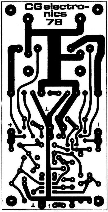
Fig.4 Single-sided PCB layout seen from below (solder side). Note that the PCB accepts both TO-3 and TO-247 encapsulated power transistors. This picture in not in scale and is shown here for reference only, if you plan to design your own PCB.
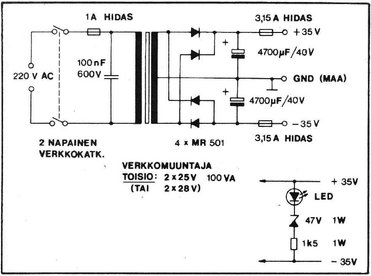
Fig.5 Suggestion for the power supply. This example is good for one channel. For stereo, you need to double the transformer power rating,, double the filer capacitors capacitance (of double their count) and use separate fuse pairs for each channel.
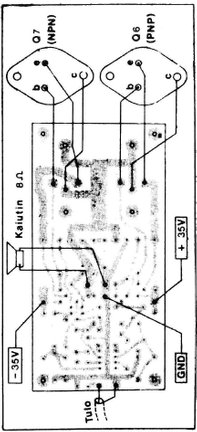
Fig.6 Wiring of the power transistors (if located remotedly), speaker output, power supply connections, and the input connection.
Parameter | Value |
Input resistance | >30kΩ |
Bandwith
| 10Hz...30KHz @ 40w |
Signal to Noise Ratio | >93dB |
Voltage gain | +34dB |
Damping factor | >50 |
THD 1kHz | 0.09% @ 100mW |
0.06% @ 10W | |
0.05% @ 40W | |
0.12% @ 60W | |
Measuerement conditions | 1kHz into 6 ohm resistive load. |
Table.2 Some basic but real-world measured parameters.
Final words and suggested improvements:
I made some crude measurements on the amplifier in 1978, they are gathered in Table 2. If you plan to design your own PCB or build this amplifier from scratch, I strongly recommend the following modifications:
- Place the ±35V fuses directly on the amplifier board. This makes the wiring easier and enables individual fuses for each amp. It also enables the following changes:
- Connect the R10 and R11 resistor power supply ends directly to the power supply lines - before the fuses. In other words, R10 and R11 should always power the Zener diodes even if the fuses are blown or missing. This is safe to do. The modification will keep the output voltage close to the ground, in case only one of the fuses has blown. The original design has the flaw that one blown fuse will produce a dc-voltage on the speaker terminals that could blow your elements before the second fuse blows. In this sense, the original design does not differ too much from many other amplifiers, many amps suffer from the same problem.
- Add a 100nF/250VAC polyester capacitor across the hot ends of the power transformer secondary wires (between the rectifying bride AC input terminals). This prevents the diodes to generate high-frequency noise when turning off on every AC cycle.
Happy tinkering!
.
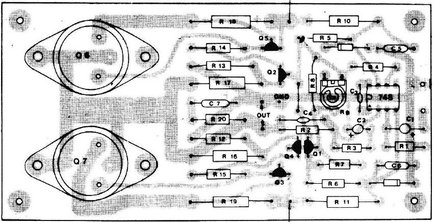
Fig.7 Component placement seen from the component side. Apologizes for the poor image quality.
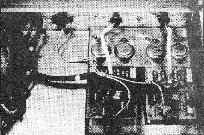
Fig.8 Stereo amplifier with the transistors mounted straight to the PCB using an aluminium bracket heatsink. Never cross the input signals (must be wired with a shielded cable) with the speaker output wiring. Keep these as separate as possible.
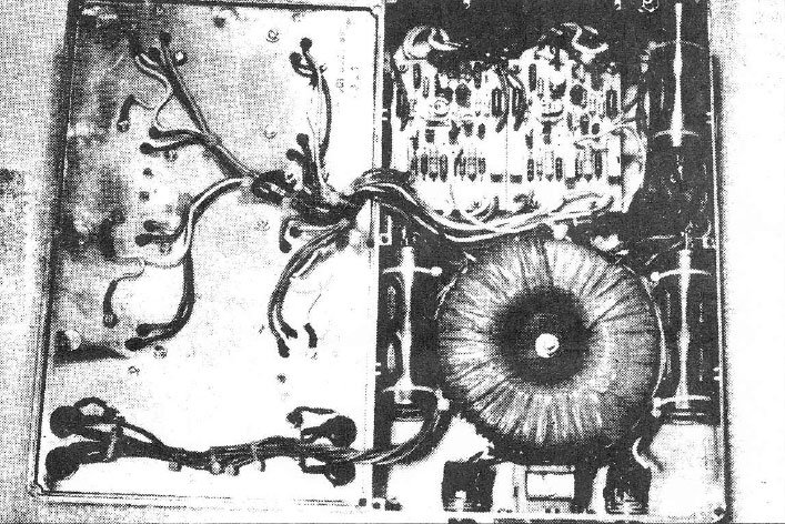
Fig.2 4-channel amplifier with the transistors mounted straight to the PCB using an aluminium bracket heatsink. Here the PCB's are slightly shortened to make them fit.
Copyright @ DEXTREL / 2023 / All Rights Reserved